SMT Stencil
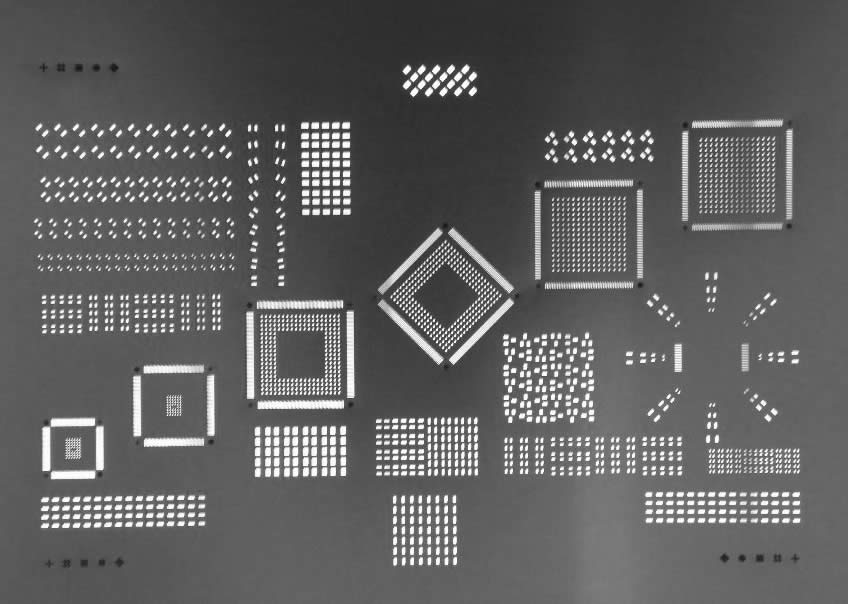
Electroformed SMT Stencils
Why Electroformed Stencils?
Precision PCB utilizes advanced Electroformed Stencils, optimizing SMT assembly with leading-edge technology.
Features & Benefits
- Electroformed SMT Stencils ensure high precision and durability, leading to consistent solder paste deposition and reduced defects in PCB assembly. This results in improved yield rates, cost savings, and enhanced overall productivity in manufacturing processes.
- Electroformed SMT Stencils offer fine detail capabilities, allowing for the creation of intricate patterns and small aperture sizes, essential for advanced PCB designs and miniaturized component assembly.
- Thinner stencils are achievable with heightened paste transfer efficiencies for improved performance.
- Custom thicknesses for stencils and foils, including variations like step-up, step-down, and recessed areas (e.g., 2.4, 4.2, 5.7 mm), are readily achievable when needed.
- The process operates at an atomic scale, ensuring micron-level aperture tolerances, typically reaching a precision of +/- 10 microns (.0004″).
- Nickel's lower coefficient of friction than stainless steel enhances solder paste roll, reducing wear on squeegee blades for smoother, more efficient operation.
- May boost production yields by reducing the need for rework processes.
- Electroform stencils expedite high aperture counts efficiently, avoiding distortion from laser heat transfer. This permits denser image areas, enhancing productivity without compromising quality, from one to unlimited pad counts.
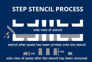
Step Stencils
Precision PCB offers Step Stencils for precise solder paste application in PCB assembly. These stencils ensure accuracy and consistency in depositing solder paste onto different PCB areas, accommodating varying component heights. By customizing stencil thickness at different regions, they optimize solder volume, preventing defects and enhancing overall assembly quality. Precision PCB’s Step Stencils guarantee efficient and reliable soldering, facilitating seamless electronic manufacturing processes.
Single Process
Through Photo Chemical Machining (PCM), our process selectively etches areas to reduce foil thickness, thereby regulating paste deposition. This precision technique ensures optimal solder volume across varied component heights, enhancing assembly quality.
Dual Process
In our dual process, we employ the Step Stencil Process, combining PCM and laser cutting for precision. Initially, PCM chemically etches areas needing minimal paste for fine pitch components. Subsequently, laser cutting ensures precise aperture creation, enhancing accuracy. This meticulous approach guarantees optimal solder deposition, enabling high-quality assembly in electronic manufacturing.
Please call our sales team at 1-888-228-9440 for a quote or to learn more information on our SMT stencils!
GET STARTED NOW 888-228-9440
For a Quick-Turn on Affordable PCB Fabrication & Assembly